

Powering the Future of Connectivity
AXT is a material science company that develops and manufactures high-performance compound and single element semiconductor wafer substrates — the critical foundation for optical connectivity, AI infrastructure, and next-generation electronic devices.
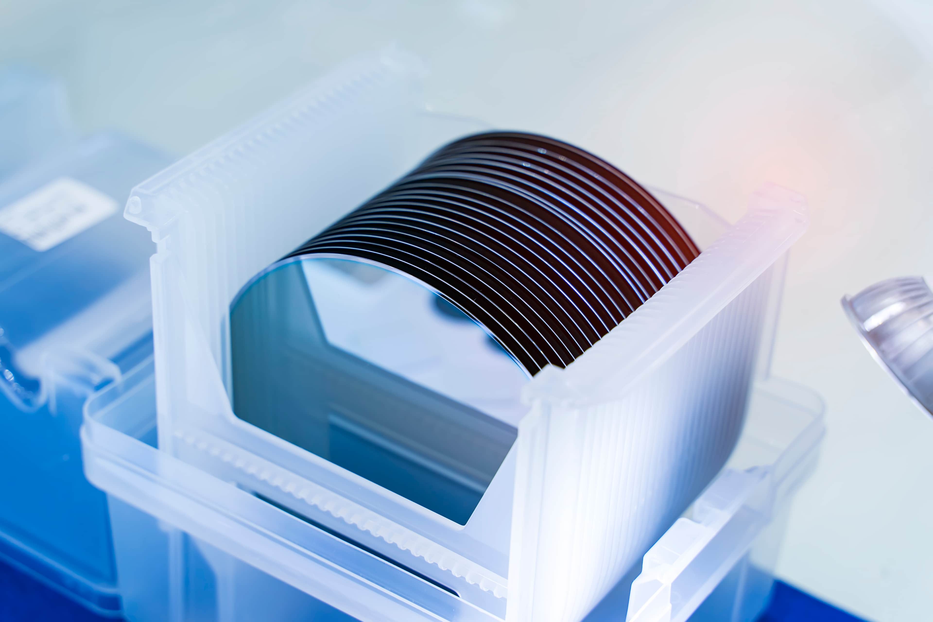
The Foundation of What’s Next
High-performance InP, GaAs, and Ge substrates — engineered at the atomic level with our proprietary VGF crystal growth technique.

Where Our Substrates Go to Work
Powering breakthroughs from AI data centers to deep-space sensing — AXT substrates serve the industries shaping the future.

Built to a Higher Standard
ISO 9001 and IATF 16949 certified processes from crystal growth to final wafer — delivering the precision our customers require.

Growing Responsibly, Operating Globally
Environmental stewardship and ethical practices across our vertically integrated supply chain.
Company Overview
AXT, Inc. (NASDAQ: AXTI) develops and manufactures high-performance compound and single element semiconductor wafer substrates comprising indium phosphide (InP), gallium arsenide (GaAs), and germanium (Ge).
Founded in 1986 and publicly listed since 1998, AXT pioneered the Vertical Gradient Freeze (VGF) crystal growth technique — a proprietary process technology backed by substantial intellectual property.
AXT is headquartered in Fremont, California, with manufacturing operations conducted through its wholly-owned subsidiary, Tongmei, which operates facilities across China.

Market Position
The compound semiconductor industry is in the early stages of a multi-year growth cycle, driven by AI infrastructure build-out and rising demand for high-speed optical connectivity.
Scale-out architectures are transitioning to 800G and 1.6T data rates, requiring high-quality InP substrates for optical transceivers.
Co-packaged optics for scale-up architectures represent the next major inflection point.
Indium phosphide is a critical material for optical connectivity, with only three high-quality providers worldwide.
AXT is uniquely positioned to expand capacity as demand accelerates.
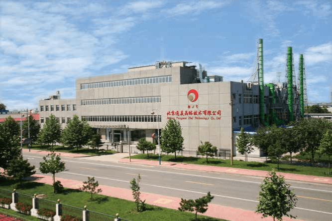
Global Operations
- Fremont, CaliforniaCorporate headquarters
- BeijingInP crystal growth and wafer processing
- KazuoGaAs crystal growth; home to two raw material joint ventures (BoYu and JinMei)
- DingxingGaAs and Ge wafer processing
Supply Chain
AXT’s vertically integrated supply chain — with ownership interests in over ten raw material companies — provides strategic advantages that few competitors can match.

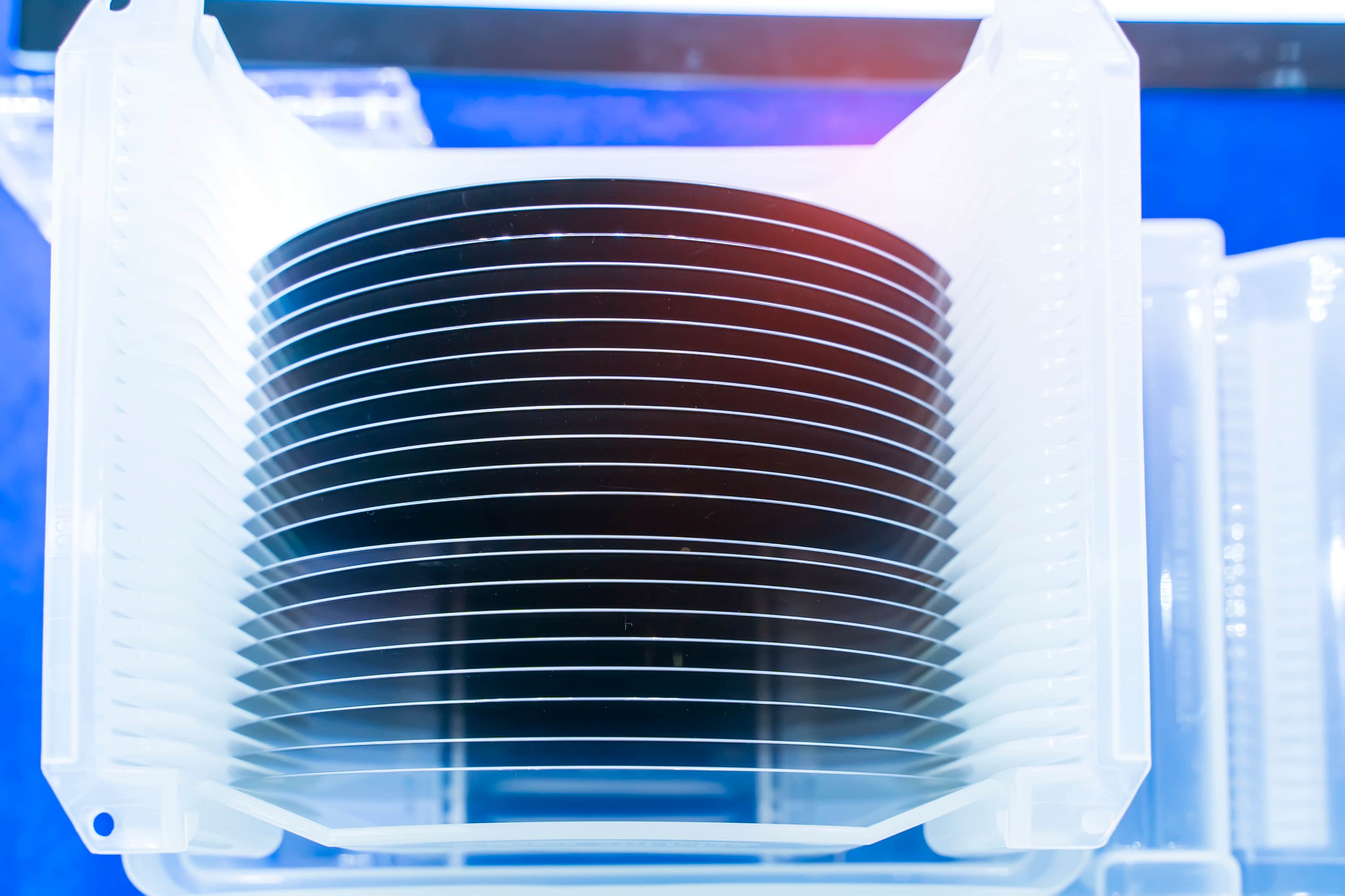
Explore Our Products
Discover our full range of compound semiconductor substrates and specialty materials.
View Products