
Semiconductor Substrates & Materials
High-performance compound and single element substrates for the most demanding electronic and photonic applications.
Product Overview
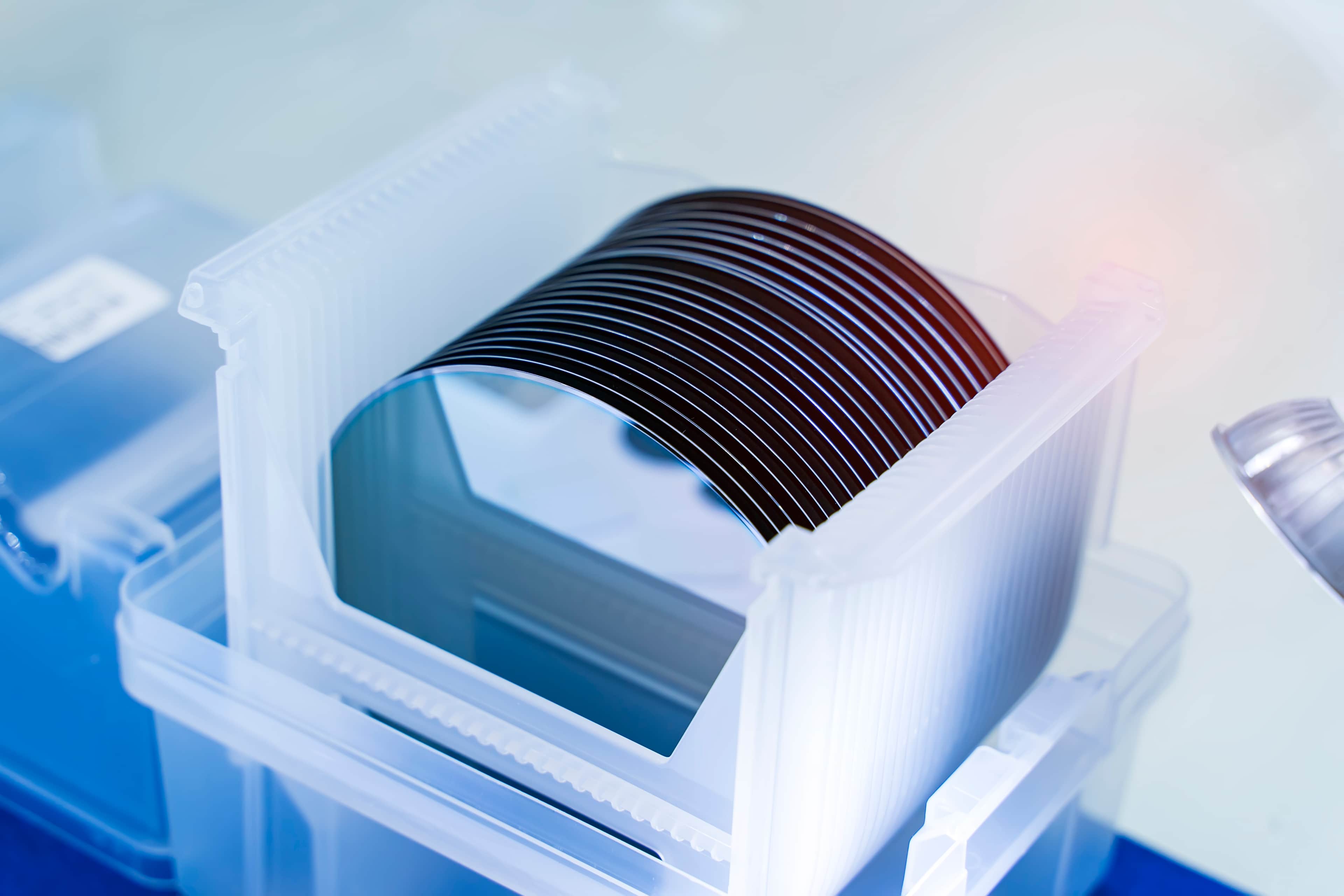
AXT manufactures three primary substrate types using its proprietary Vertical Gradient Freeze (VGF) crystal growth technique, alongside specialty raw materials that support both internal and external customers.
Indium Phosphide
The material of choice for high-speed optical communication, AI data center interconnects, and advanced sensing applications. AXT is one of only three global providers of high-quality InP substrates.
Available Diameters
Available Doping
Applications
- Optical transceivers
- Co-packaged optics
- Silicon photonics
- High-speed lasers & detectors
- 5G & telecom infrastructure
- Autonomous vehicle sensing
Gallium Arsenide
Serving a broad range of electronic and photonic applications, from wireless communications to advanced display technologies.
Available Diameters
Available Doping
Applications
- Cell phone power amplifiers
- VCSELs & 3D sensing
- LED lighting & display
- MicroLEDs
- LIDAR
- RF devices
Germanium
Essential for high-efficiency multi-junction solar cells and serving as carrier bases in wafer fabrication lines.
Available Diameters
Available Doping
Applications
- Satellite solar cells
- Carrier base substrates for wafer fabrication
Raw Materials
PBN (Pyrolytic Boron Nitride) Materials
Critical components in semiconductor crystal growth and processing equipment — including crucibles, plates, coatings, and boron oxide.
High-Purity Materials
Ultra-high-purity materials essential for compound semiconductor manufacturing, including high-purity gallium and specialty alloys.
See Where Our Substrates Are Used
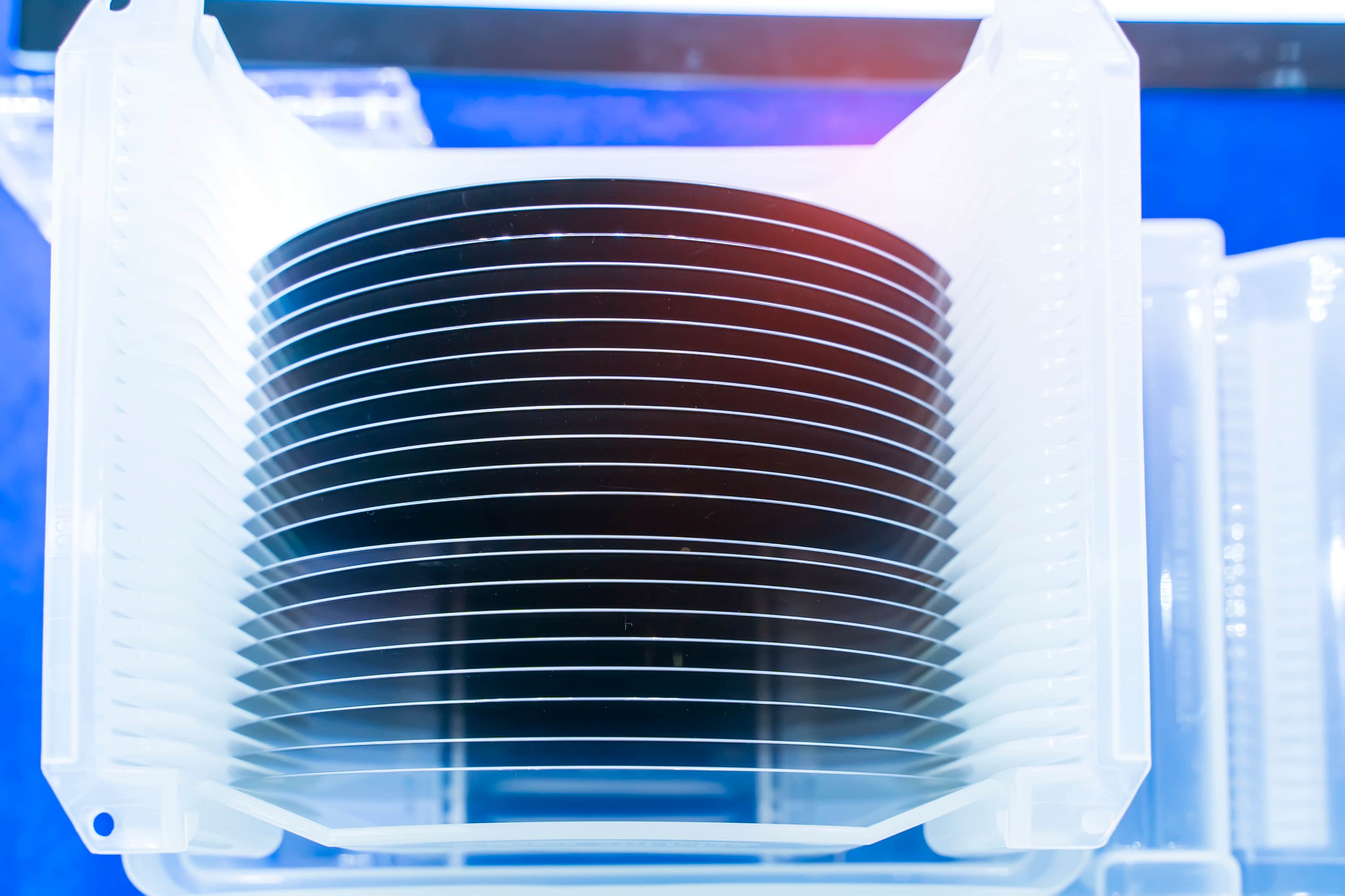
Explore the industries and technologies powered by AXT compound semiconductor substrates.
See Our Applications