Submitted by drupaladmin on Thu, 2006-02-09 02:29.
A direct consequence of the relatively low defect density in VGF grown GaAs substrates is the increased mechanical strength of the material. Substrates with a high dislocation density can easily form microcracks where the dislocations coalesce. An almost linear increase in wafer fracture strength, with decreasing dislocation density, has been observed. High mechanical strength is desirable, because it results in reduced wafer breakage during volume processing. It also allows the use of thin wafers during processing, eliminating the thinning steps often required for devices. The superior mechanical properties of GaAs VGF grown substrates lead to a unique AXT feature - extra thin 100µm-thick wafers.
The relationship of structural imperfections of epitaxial layers to their substrates has been closely examined by Bassignana and Macquistan1. Layers of 2-µm thick Al.5Ga.5As were grown by conventional molecular beam epitaxy (MBE) and metal-organic chemical vapor deposition (MOCVD) on LEC GaAs semi-insulating substrates. Studies showed that all the threading dislocations associated with the dislocation cellular network in the substrate extend up into the epitaxial layer in exact one-to-one correspondence. This dislocation propagation exists in both MBE and MOCVD growth. Hence, a higher quality substrate is a primary condition for obtaining a high quality epilayer.
Although the dislocation density of the substrates has been shown to strongly affect the quality of epitaxial layers, a common claim is that it has no definite effect on the device's performance. Decisive effect on device performance has been found to be related to AB defects2, although the origin of AB defects is not well understood. These defects can be revealed by AB solution etching as oval defects, and are generally believed to be As precipitates. Field-effect transistors (FETs) with more AB defects exhibit poorer performance and uniformity. In VGF grown GaAs substrates, the AB defect density may be orders of magnitude lower than in GaAs substrates grown using the LEC technique, and therefore such VGF grown GaAs substrates are more suitable for these epitaxial devices.
| High Defect LEC Substrate | Low Defect VGF Substrate |
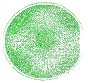 | 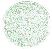 |
Figure A Defect density can vary greatly with 3" substrate
Recent systematic studies at TRW further show that MBE layers grown on VGF substrates have significantly better surface morphology, with much lower defects and haze, than those grown on LEC substrates3. The improved surface morphology translates directly to higher circuit yields. Figure A compares surface scan results of 76.2 mm MBE layers grown consecutively on these substrates. Epitaxial growth of model InGaAs/GaAs high-electron-mobility transistor (HEMT) device structures at TRW yielded similar results. As shown in Figure B, the HEMT epitaxial layers on VGF substrates have decade lower defect density than on LEC substrates. It should also be noted in Figure B that LEC substrates inserted in the VGF series show the same results as the earlier LEC series.
TRW also showed that transmission electron microscopy (TEM) reveals partial relaxation of the strain and a dislocation density of ~4500 cm-2 for structures grown on LEC substrates, while no relaxation and dislocation are observed on structures grown on VGF grown substrates. The TRW study concluded that the critical thickness of pseudomorphic InGaAs/GaAs HEMTs is greater on VGF than on LEC substrates. In addition, photoluminescence measurements show greater intensity for HEMT structures based on VGF grown substrates. Measurements of transconductance and channel resistance, as a function of channel thickness in HEMT structures, show that improved device performances on VGF grown substrates are more obvious with increasing channel thickness. TRW concluded that by using VGF grown substrates, better yield, epi-layer quality and device performance can be achieved on the production line than if LEC grown substrates had been used.
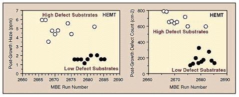
Figure B High GaAs substrate defect densities translate directly to higher HEMT epi-layer surface defects
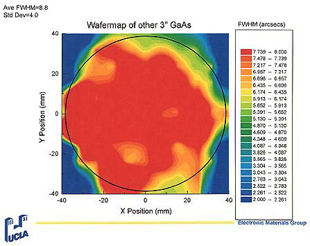
A four crystal x-ray diffraction mapping of the x-ray Bragg angle distribution of VGF and LEC substrates has been made by Prof. Goorsky at UCLA. Figure C shows the typical Bragg angle distribution of a 3" LEC grown substrate. In contrast, Figure D shows the Bragg angle distribution of a 3" VGF grown substrate. The average FWHM of the LEC grown substrate is 8.8 arc seconds. The average FWHM of the VGF grown substrate is 3.8 arc seconds. However, the standard deviation of the FWHM of the VGF grown substrate Bragg angle distribution is an order of magnitude better than that of the LEC grown substrate - 0.4 arc seconds vs. 4 arc seconds. This study demonstrates the superior crystalline quality of the VGF grown substrate.
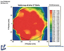
Figure C | 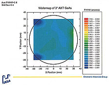
Figure D |
- I. C. Bassignana, and D. A. Macquistan, in Common Themes and Mechanisms of Epitaxial Growth Symposium, Edited by: P. Fuoss, et al. (San Francisco, 1993), Mater. Res. Soc. 1993, p. 185.
- H. Yamamoto, O. Oda, M. Seiwa, M. Taniguchi, H. Nakata, and M. Ejima, J. Electrochem. Soc. 136, 3098 (1989).
- D. C Streit, T. R. Block, M. Wojtowicz, A. Han and M. Goorsky, 16th North American Conference on Morelcular Beam Epitaxy Oct 5-8, 1997.
|